Introduction
The DFT -1/2 method
DFT-1/2, an alternative way of referring to the LDA -1/2 [1] [2] and GGA -1/2 [2] techniques, is a method for approximate self-energy corrections within the framework of conventional Kohn-Sham DFT which can be used not only with the local density approximation (LDA), but also with the generalized gradient approximation (GGA) [11] [2] [12].
The method aims to predict energy gaps results with the same precision [2] as the quasiparticle correction [9] algorithm, considered the state of the art for calculating energy gap of semiconductors. In addition, the computational effort of the method is equivalent to the standard DFT approach and and is three orders of magnitude lower than the aforementioned GW method [16] , which allows the technique to be applied to complex systems.
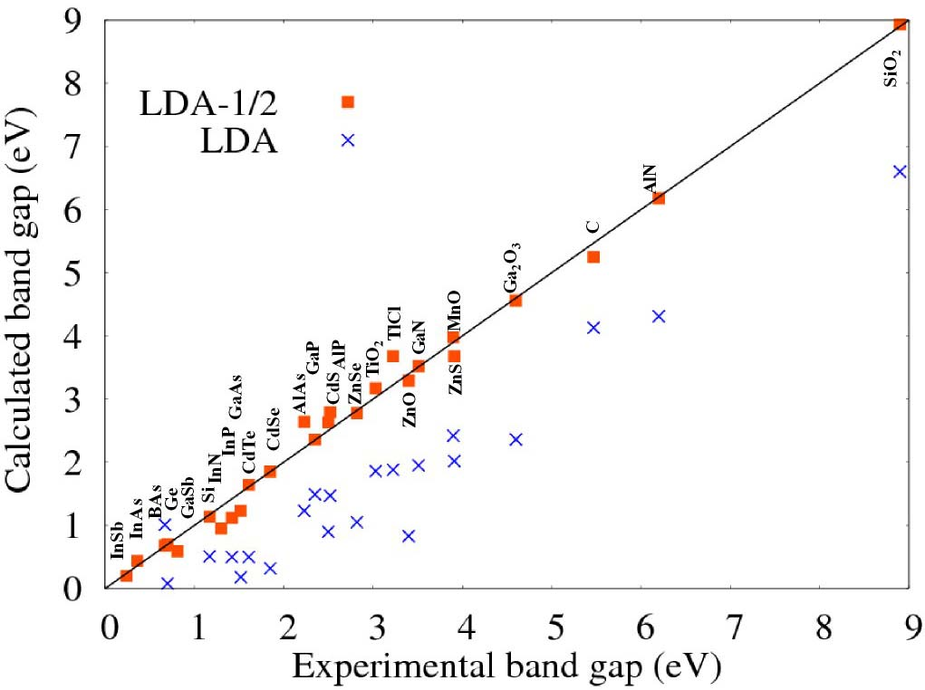
Fig 1. Comparison of calculated band gaps with experiment. The red square are the SCF LDA-1/2 (standard LDA-1/2). The crosses are standard LDA. The small gap semiconductors are metals (negative gaps), when calculated with LDA. LDA-1/2 corrects the situation. The band structure calculations were made with the codes VASP [13] [14] and WIEN2k. [15] [2]
What is minushalf?
Minushalf is a command line interface (CLI) developed by the group of semiconductor materials and nanotechnology (GMSN) that aims to automate the application of the DFT -1/2 method. The commands available in this CLI automate both the entire process and each of its steps in order to be used for several purposes.
An intuitive explanation of the DFT -1/2 method
This method aim to expand the half-occupation technique [3] [4] [5], formalized by Janak’s theorem, to crystals using modern exchange-correlation approaches [6] [7].
The Slater half-occupation scheme has already proven to be quite efficient for calculating atomic ionization energies values close to the experimental ones [5]. However, this technique cannot be applied blindly to extended systems like crystals, since the crystal is described by means of Bloch waves and removing the population of just one Bloch state would have no consequences [1]. Moreover, removing the population of one Bloch State and set periodic conditions would result in a infinitely charged system.
Thus, the proposed solution is to apply the Slater procedure to crystalline energy bands. The intuition for this application comes from the fact that the energy bands of a crystal are formed by the overlap of atomic orbitals, mainly by those that constitute the outermost layers [8]. This relationship can be quantified by the projection of the wave function in a given orbital, Figure 2 shows the \(p\) character for each atom in the band structure of the h-BN, the bigger the blue dots, the stronger the character. Thereby, considering this existing relationship, self-energy corrections performed in atoms could propagate and shift the energy of the bands, resulting in a band gap correction.

Fig 2. \(p\) character for each atom in the h-BN band structure. The bigger the blue dots, the stronger the character.
How to perform potential correction in crystals
In this section, calculations were developed using some approximations in order to demonstrate intuitively how the potential correction in crystals is made. To access the rigorous demonstration, consult the references [1] [2] .
Following the Slater half occupation procedure for atoms, a change in charge density is required to obtain the potential for semi-occupation and perform the consistent calculations using the Kohn-Sham equation.
Altough in extended systems like crystals a change in charge density in a unit cell would result in an infinitely charged system, which would lead to a divergence in the Kohn-Sham calculations. Furthermore, it would also be irrelevant to be able to modify only a finite amount of electrons in the crystal since the charge would become irrelevant to the infinite amount of electrons present in the system. To bypass this problem, it is necessary to find a new way to derive the semi-occupied potential.
Firstly, one have to define the system that corresponds to the semi-occupied potential for a solid. For an atom containing \(N\) electrons in its ground state, the semi-occupied potential is defined as the potential of the atom with \(N-\frac{1}{2}\) electrons. Similarly, we should consider that the semi-occupied potential of a solid would be the potential generated by a solid with \(M-\frac{1}{2}\) electrons per primitive cell, where \(M\) is the number of electrons of the unit cell in the ground state, as shown in Figure 2.

Fig 3. Scheme representing the unit cells of a solid that would generate the potential semi-occupied.
So, to outline the solution, suppose one have \(N\) independent charge distributions, where the \(mth\) is given by:
Where \(\rho\) represents the density of the distribution \(m\), \(q\) represents the charge of the electron, \(\eta\) a normalized function in space and \(f\) represents an occupancy factor that varies continuously from 0(occupied) to -1(unoccupied).
Considering the charge density represented above, one can find the Coulomb potentials for each distribution by the Poison equation:
Now, suppose another situation where one only alternate the occupation of the \(\alpha\) level and the same charge distribution remains. In this scenario, the \(mth\) potential is given by:
Thus, one want to calculate the potential for all distributions, which is obtained by adding of the potential of all distributions, as shown in the equations below.
Subtracting these two equations:
Using the above equation for the specific case of \(f_{\alpha} = 0\) and \(f_{\alpha}{'} = -1/2\), the following equation is obtained:
Hence, using the equation above, one can calculate the potential semi-occupied from other potentials, which discards the need for modify the charge density. For a crystal, the equation is written as follows:
Where \(V_ {crystal}^{- 1/2}\) is the potential of the semi-occupied crystal, \(V_ {crystal}\) is the potential of the crystal in the ground state and \(V_ {1 / 2e}\) is the potential of the respective level occupied with half an electron.
There is a problem with adding \(-V_ {1 / 2e}\) to all the atoms of an infinite crystal: the potential will diverge. \(-V_ {1 / 2e}\) is a potential of an excess charge of 1/2 proton and has a tail of 0.5/r that cannot be summed in an infinite lattice. Therefore the tail has to be trimmed by a step function [2]. Besides, it is worth mentioning that the values for \(CUT\) and \(A\) must not be chosen arbitrarily, by means of variational arguments it can be proved that the optimal values for these parameters are those that maximize the band gap of the crystalline system [1] [2] , as shown in Figure 3.
Hence, to obtain \(V_ {1 / 2e}\), the following equation is used for the atoms that compose the crystal [1] [2]:
Where \(V_{atom}\) is the potential of the atom in the ground state, \(V_{atom}^{f_{\alpha}=-1/2}\) is the potential of the atom with the level \(\alpha\) occupied, \(\theta (r)\) is a trimming function, CUT is the cut radius and A is a scale factor named amplitude.
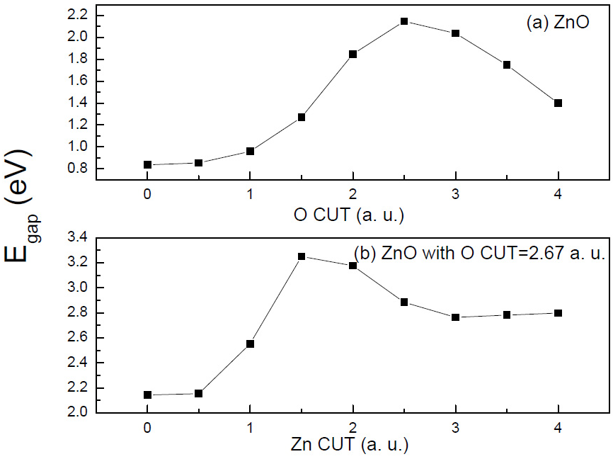
Fig 3. The figure depicts the choice of \(CUT\) for \(O\) and \(Zn\) in the case of \(ZnO\). First we maximize the gap varying \(CUT^{O}\) , then we vary \(CUT^{Zn}\) to reach a band gap value near the correct value [2].
Finnaly, since the atoms repeats in each unit cell, the potential \(V_{1/2e}\) is periodic, joining this information with the fact that \(V_{crystal}\) is periodic, one can conclude that \(V_{crystal}^{-1/2}\) is periodic, which implies that the boundary conditions remain periodic and the Kohn-Sham calculations can be applied to the system.
The CUT parameter
As observed for several 3D and 2D materials [2] [12], one may observe that a \(CUT\) parameter has a strong dependence on the considered element where the half occupation is applied, as shown in Figure 4 for two-dimensional materials, which is consistent with the environment neglect and the isolated atom approximation for the self-energy potential.The significant differences between CUT parameters for one element in distinct materials is explained by the difference between bond lengths in the studied materials. In general, materials with smaller first-neighbor lengths exhibit smaller cutoff parameters. A linear relation between the \(CUT\) parameter and the bond lengths (d) is observed for several classes of 2D materials [12] and 3D materials [1].
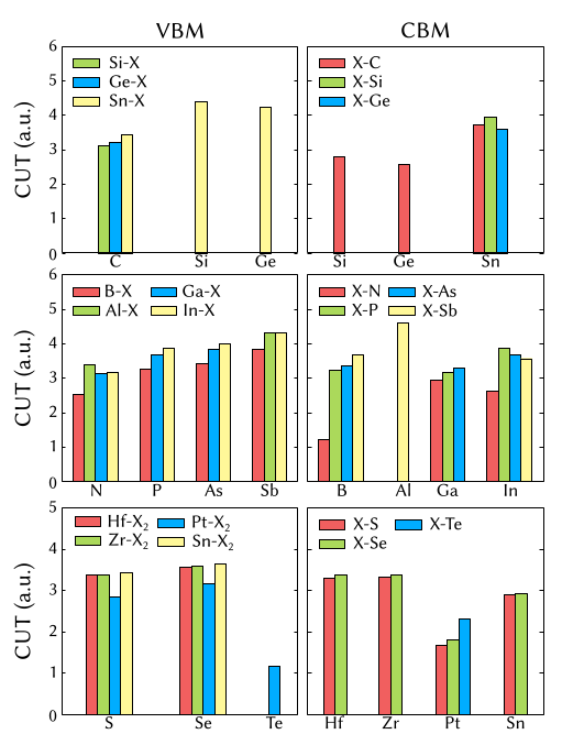
Fig 4. Cutoff parameter comparison for a selected set of 2D materials. The cutoff parameters of the VBM (CBM) states on the anions (cations) are represented on the left (right) [12].
Where to perform semi-occupation?
There are two types of correction, simple and fractional, and they must be performed in the last valence band (\(VBM\)) and the first conduction band (\(CBM\)). The choice of which correction cannot be made blindly, it requires an analysis of the band’s composition. To explain these two corrections, suppose that we have a matrix where the atoms of the unit cell are represented as lines and the types of atomic orbitals \((s, p, d, f ...)\) as columns , each value \(a_{ij}\) represents, in percentage, how much that orbital \(j\) of a given atom \(i\) contributes to the total module of the wave function.
Where:
Simple correction
The simple correction method is applied when an index \(a_{ij}\) mainly represents the composition of the band, so that the influence of the other orbitals is negligible. Thus, the correction of half an electron is done only in the orbital \(j\) of the atom \(i\).
Fractional correction
The fractional correction method is applied when different atomic orbitals have a significant influence in the composition of the band, it can be observed in the conduction bands of Figure 5, where the \(p\) and \(d\) orbitals compose the band simultaneously. To distribute half an electron, a threshold is chosen \(\epsilon\), which represents the minimum value of \(a_{ij}\) considered in the correction. Given these values,the half an electron will be divided among the atoms, proportionally to the coefficient \(a_{ij}\).
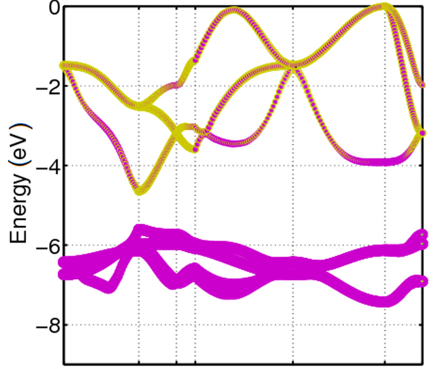
Fig 5. Orbital character for CdO valence bands. The character \(p\) is represented in yellow and the character \(d\) in a magnet [10].
Is conduction band correction always necessary?
In many cases, the correction in the valence band already returns satisfactory and close enough results, which rules out the need for an additional correction in the conduction band.
Final considerations
After applying the correction, the optimum cut must be found for each corrected atom to find the final value for the gap.